uTracer3+, improved switch performance
- bob6542
- Nov 23, 2024
- 10 min read
Updated: Nov 26, 2024
The uTracer3+ provides great value for your money.
In it's stock form I have found the uTracer3+ is a reliable if not somewhat limited unit.
The stock uTracer3+ is limited to a maximum Va and Vs of 400V with a maximum test current of about 200mA.
While the stock maximum current level of 200mA covers a lot of tubes the 200mA current limit does prevent many power tubes from being investigated fully.
As well in order to use the full 200mA current capability a protective measure called "compliance" must often be turned off. With compliance turned off a short, arc over or over load puts the uTracer3+ switches used to apply Va and Vs in great danger of damage.
There is a modification published by Ronald the utracer3 designer to extend the uTracer3+ to a 600mA test capability. This modification does nothing to make the switches more robust.
The result is a uTracer3+ with the 600mA modification is a far less robust unit where switch failures occur too often.
The switch circuit used to control Va and Vs is a very dated design using a number of older BJT high voltage PNP devices.
Ronald's uTracer3 design has little margin in the switches at high currents.
The safe area of the KSA1156 is only Vce=25V @ Ice=650mA
See attached picture of switch safe area below
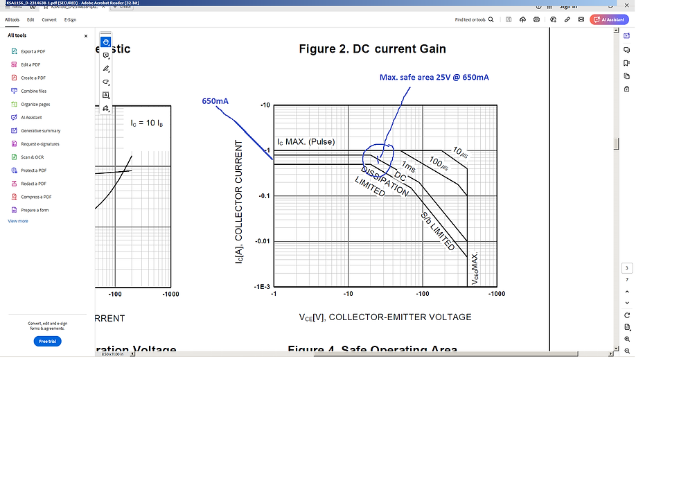
The above shows the safe area for the uTracer3+ KSA1156 switch BJT.
To make the danger larger Ronald's design only limits current in the switch and does not protect the switch based on the safe area (Vce * Ice)
This means when the hardware current limiter is active the switch is in great danger of overload and failure as the current stays high and the Vce keeps rising on each measurement until the switch fails from safe area overload.
With compliance turned on the PIC shuts down the switch in under 10uS and provides a second chance for the switch. This works well with the stock 200mA uTracer3+.
However with the 600mA modification even with with compliance turned on switch protection is marginal. This again is related to the limited safe area of the KSA1156 switch used. If you review the KSA1156 safe area chart at 10uS and 400V the limit for current is about 400mA. That is a problem for a switch with the hardware current limiter set to over 700mA as is the case for the 600mA modification for a utracer3+
Personally I never design past the data sheet safe area values for a BJT due to the high risk of failure although some designers do.
The the uTracer3 switch driver a PN5416 transistor is limited to Vceo of 300V and a Vcb of 350V yet must withstand over 400 volts. I see this like living on borrowed time.
Finally both the PN5416 and KSA1156 are now listed as end of life.
There must be a better way forward.
A new uTracer3+ switch design.
I took a page from the uTracer6 switch design that uses a modern N channel MOSFETs for the switch in place of the old PNP BJT.
My target was a 1A uTracer3+ test current so the switch will be set to limit current at about 1.2A.
I selected a MOSFET that by the data sheet can withstand 4.1A at 400V for 1mS.
This MOSFET should easily withstand a full 1.25mS pulse at 1.2A and 400V with no protection needed from the compliance function.
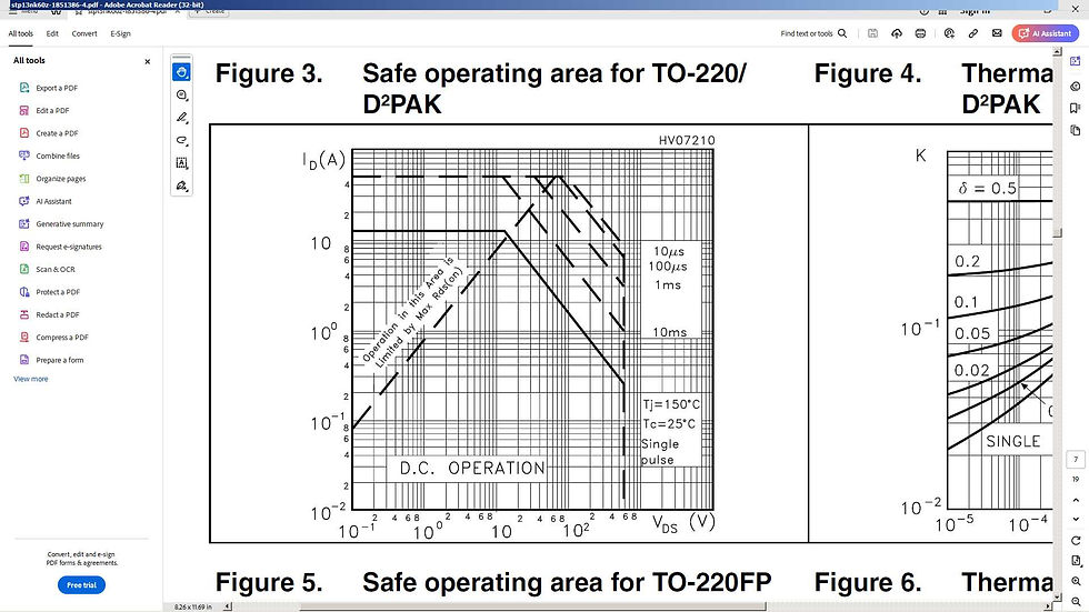
The STP13NK60Z MOSFET and it's safe area.
Note the 1mS pulse duration line on the right side at the 400V intersection is 4.1A current.
A design based on the above MOSFET by the data sheet should be basically bullet proof at a 1A test current and 400V even with compliance turned off.
Based on the above I designed, built and tested a new PCB based on the STP13NK60Z MOSFET.

Above is the first version of the improved uTracer3+ switch.
I proved to be a excellent power oscillator for a few seconds time.
I set the current limited to 200mA.
On lab testing into a 4 ohm load (close to a dead short) at a 200mA current limit all was well and the switch worked as designed.
I reset the current limiter to 600mA.
Testing at about the 500mA level with only about 15V applied I saw the regulated power supply voltage rise rapidly and the switch module failed.
Trouble shouting the failure I found the OPTO coupler IC a TLP2745 had shorted. The explanation seemed it failed due to over voltage when the power supply voltage rose for no apparent reason.
Ok that was weird.
I know from experience when strange excess voltages appear in high speed/current circuits it is often a sign of instability, ringing or oscillation. Sitting I looked at all the connection leads and considered all the little inductors that were sitting there. Lots of inductance to ring or resonate with the capacitance in a power MOSFET and generate high voltages if allowed to do so.
I went back the the spice simulations and added some inductance. 10uH or so.
Oh my what a mess my nice clean pulse became with 10uH added.
Sure enough high voltages were the result in the switch circuit with oscillation at many 100Khz. I though Ok just shorten up the bench leads and all will be be well.
A quick look at the uTracer3+ circuit diagrams showed there are added inductors in series with both the anode and screen leads. Then there will be all the wiring to the many sockets that uses will add. So it was clear I needed a switch circuit that would operate correctly in the presence of lots of stray inductance.
A added 50uH of inductance the amount built into the uTracer3 main board and the spice results we not surprisingly even worse for my new switch design.
I though "that stock switch uTracer3+ circuit must be a pretty tricky piece of design to work perfectly with all this added inductance".
So I built the present uTracer3+ switch circuit in spice to allow me to simulate it.
At the stock 200mA current limit spice showed the stock switch design worked pretty well much like my first design had at 200mA.
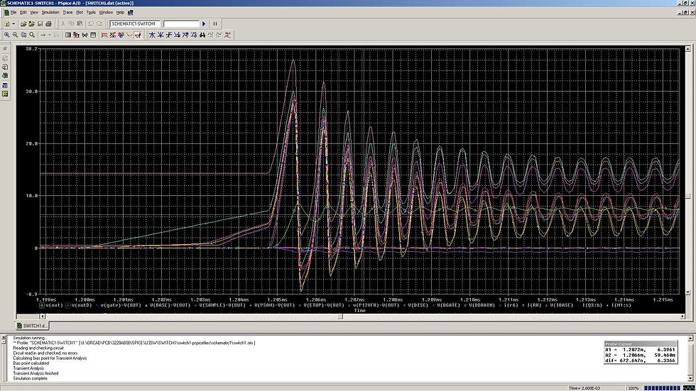
When I increased the current limit to 600mA and simulated a 1 ohm short circuit all hell broke loose in the stock uTracer3 switch circuit. Huge destructive voltages and strong oscillation was the result. It seemed very unlikely the KSA1356 switch would survive a full voltage current pulse into a dead short no matter how fast the software shut things down.
I felt a little better about my circuit's quick death at 500mA.

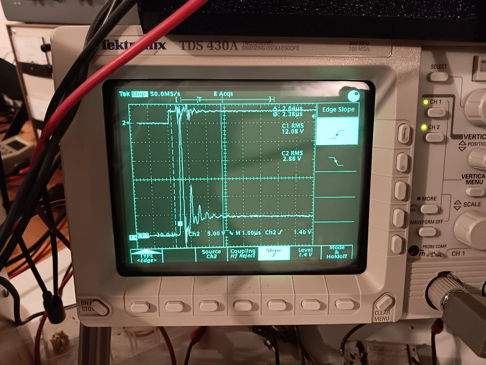
Stock utracer3 Switch turn on 600mA. Oh my the ringing voltages
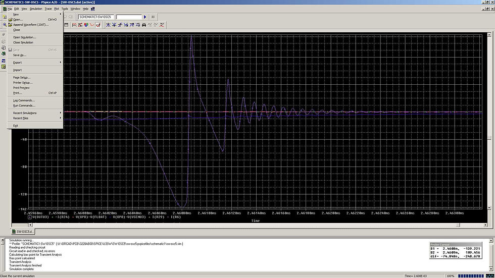
Stock utracer3 Switch turn off 600mA. Nasty voltage undershoot with turn off.
Remember the uTracer3 switch is already marginal on rated voltage without a added undershoot of 150 volts more.
Back to the drawing board.
Thinking on this puzzle the requirements for this circuit are contradictory.
There is the need to turn on and off the switch quickly so the tube under test is ready when the software starts to make measurements. As well a slow switch turn on and off causes a lot of power to be dissipated in the switch for each transition.
But then the stray inductance argues for slow transitions to prevent ringing and voltage over shoot.
Yet more complex the current limiter function has to be able to act at the turn on speed or faster to limit the maximum current effectively. Then the switch circuit must smoothly transition into a linear current regulator that is stable with a inductive load now suggesting a slow speed current limiter was needed for stability.
All this contradiction seemed a tall order to satisfy. I went for a walk.
Back to spice for a lot of what if's.
After many failed or marginal versions I seemed to have a circuit that met the above requirements.
At a measurement pulse start he new design drives the MOSFET gate at high current (but not too high) for a fraction of a uS , to place a lot of charge on the gate and get the MOSFET switch nearly fully on. The turn on gate current is however limited as we do not want to induce too much ringing in the stray inductance by a really fast rise time.
The TLP2745 opto coupler I used has only about 100nS logic delay unlike the 4N25 with its many uS of delay.
This affords the new circuit the luxury of allowing slower rise and fall times for the MOSFET to limit ringing while still getting the MOSFET fully on and fully off in the same total time as the original design. The very robust MOSFET I selected allows me the luxury of not being overly concerned if the MOSFET spends a few uS turning on and off.
A second benefit of using a modern high speed opto coupler is that the TLP2745 only required 1/10 the drive current from the PIC I/O port that is required by the two 4N25 opto couplers. This means the pesky rise in grid voltage that troubles the uTracer3 due to PIC internal ground bounce will be finally be totally banished.
Once we have a good gate charge stored on the MOSFET gate the MOSFET drive circuit transitions to a low gate drive state to allow a slower current limiter loop response in case the current limiter comes on into a too low impedance and needs to limit the MOSFET maximum current. If the current limiter was allowed to continue to operate at high gate drive currents the fast loop response will lead to instability in the presence of all the external inductance. A 1.2A current oscillation at a few 100Khz backed up by a 400V power supply into a 50uH inductance can product a frighting high voltage.
The turn off gate drive current has a separate drive path to allow the turn off gate drive to be tailored to limit ringing and over shoot in the external inductance at turn off.
Even with all the above there is still need for further measures to prevent large fly-back voltages from be developed by the external inductors.
One case is if the output connections are loose and the test current is broken during the test pulse all my careful control of the switch's turn off time will be of no help and the stray inductance will flyback producing a large voltage spike. Bang is the likely result.
I took two measures.
First a high speed damper diode is added with diode cathode to the switch output and diode anode to ground BEFORE the fuse and inductors La and Lb. This is done for both the anode and screen switches.
The result is any flyback voltages from stray inductance will be shunted by the damper diodes harmlessly to ground.
The second measure is to reduce the Q of the added inductors La and Lb. This is done by bridging each inductor with a 1k 1/4 resistor. The 1k resistor still allows the inductors to provide rise time control and lower the likelihood of a tube oscillation. The reduction in inductor Q will likely also improve damping of tube oscillations.
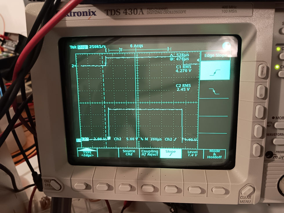
The result of all of the above was very nicely controlled turn on and turn off edges testing at the full 400V level into a 500 ohm load (about 800mA) pulse.
I made a simple Arduino based controller to simulate the uTracer3's PIC's signals for testing.
No uTracer3s were harmed in this development effort!
See the scope photos.

1.25mS pulse into 500 ohms at 400V. Nice and tidy pulse

Rising edge into 500 ohms at 400V. Notice there is zero bounce or ringing

Falling edge into 500 ohms at 400V. Notice there is zero bounce or ringing
Below are tests into a over load I used 4 ohms and 8 ohms at 400v test voltage.
The switch had no problem surviving repeating pulses into these loads at a 400 volt test voltage. Compliance is no longer required for switch safety.
Full 1.25mS pulse into 4 ohms with a 400V test voltage. The switch is fine with repeated testing. The pulse shape is nicely formed at a 1.2A current level limited by the MOSFET
The leading edge into 8 ohms. There is only limited ringing caused by the external inductor La.
The switch circuit stayed stable.

The falling edge into 8 ohms. There is limited ringing caused by the external inductor La.
The ringing is low in amplitude at a only a few volts.
The switch circuit stayed stable.

Full 1.25mS pulse into 1 ohm with a 400V test voltage. The switch is fine with repeated testing.
The the 1.28V voltage pulse across the 1 ohm resistor shows a nicely formed current pulse at a 1.28A current level limited by the MOSFET.
There is no visible under or over shoot in current.
The spice results for the circuit shown above and below seems to address all of the issues.

Finial circuit for the improved switch into a short shows almost no leading leading edge ringing

Finial circuit for the improved switch into a short shows almost no trailing edge ringing
Finial circuit for the improved switch.

Lab testing showed the improved circuit was stable and would easily withstand repeated test pulses into a short at 400V and 1.2 amps test current.
The leading edge shows a small amount of inductive ringing that quickly damped out.
The falling edge was very clean.
Lets see what happens at 500 volts
Since I was finished testing the switch I thought lets see what happens at 500 volts.
The data sheet suggests the MOSFET should be fine at 500V @1.2A for 1.25mS.
There is a question of creepage and clearance for 500 volts that I admit I did not look at as this was a 400V design.
Lets see anyway what happens.
I did the testing into a 1 ohm short circuit with the current limit set to 1.2A and full 1.25mS pulse. Pretty mean test.
At 450V all was fine and the pulse current looked unchanged. Same for 475V still looking good.
At 485 I was getting nervous but all still looked fine.
At 495V it produced a nice loud bang. The MOSFET shorted, the opto coupler shorted and most of the resistors exploded. Oh well.
It is not clear what caused the 495V failure and more study will be needed.
It does suggest that at uTracer3 voltage levels of 400V we should be fine with good margin.
Getting to 500V may be a future project when I have a bunch of modules to kill off of the next revision.
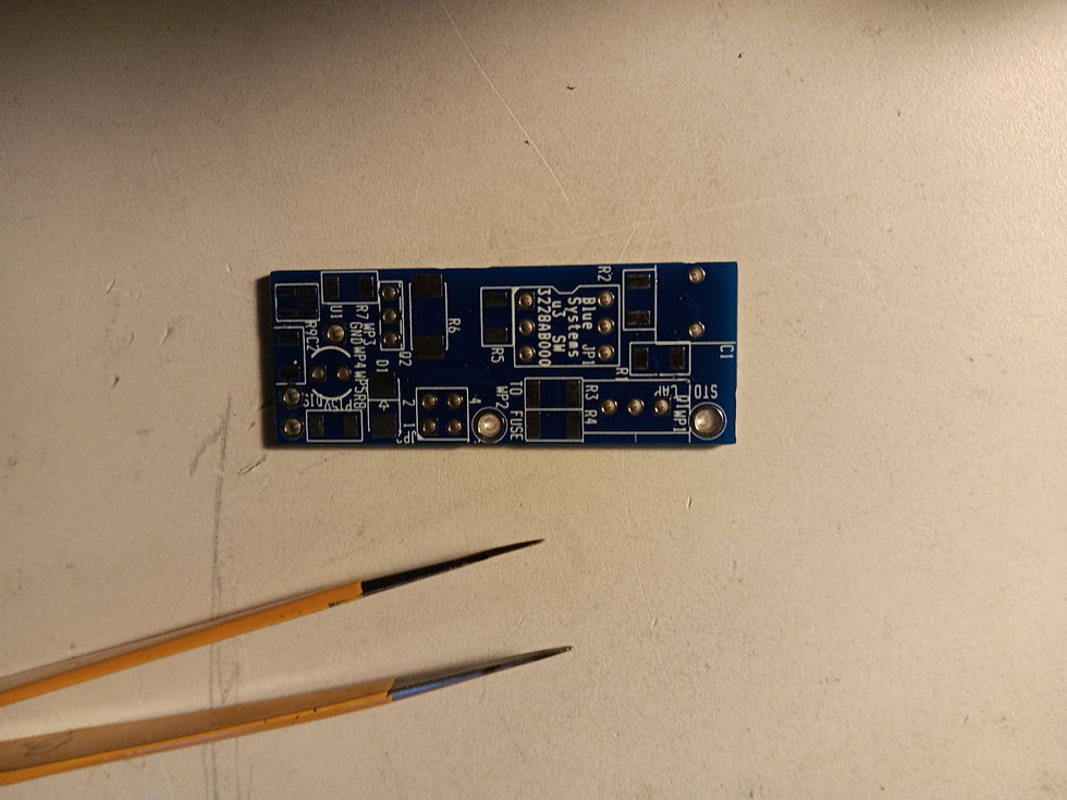
Here is the PCB for the improved switch.
This is the early version and will now need a revision for the improvements.
The PCB will plug into the opto coupler socket and attaches with 4 additional wires.
It is designed fit between the large storage capacitors plugging into the opto socket on the uTracer3 board. It has jumper select-able current ranges of 200mA , 600mA and 1A.
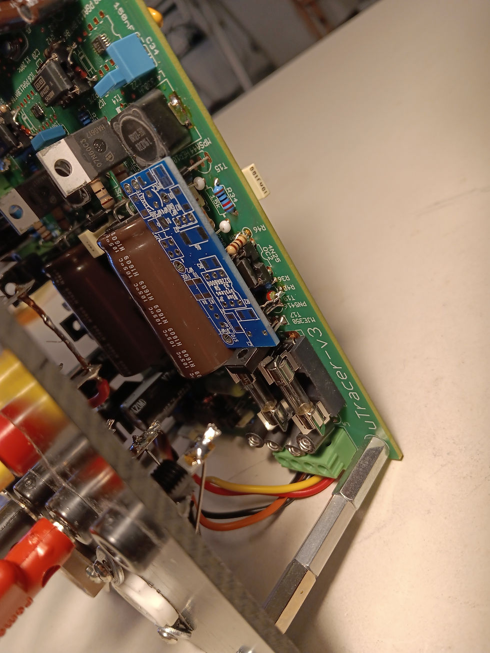
Sits nicely in-between the large storage capacitors.
When the next revision PCB has arrived and is tested I will put up the design for anyone to use.


Comments